
Hardware · Embedded Systems · Prototyping
Integrating CAD, 3D Printing & Software Building Smart Prototypes That Actually Work
Building a connected hardware product means running three disciplines simultaneously — CAD, electronics, and software. The teams that do it well treat all three as a single workflow from day one, with deliberate handoff points rather than a chaotic integration sprint at the end.
Start With a Unified Design Brief
Writing separate briefs for the physical and digital components is the most expensive mistake you can make early in a smart product project. Your mechanical team designs a clean enclosure, then your firmware developer realises there’s nowhere to route an antenna. The software team builds an elegant BLE stack, then discovers the chosen microcontroller doesn’t have enough flash to run it.
A unified design brief forces these questions to the surface before anyone opens a CAD file or writes a line of code:
What is the device doing physically?
Sensing, actuating, displaying, dispensing? The physical function determines PCB real estate, power draw, and how mechanically demanding the enclosure design will be.
What are the connectivity requirements?
WiFi, BLE, LoRa, cellular, wired Ethernet? Each protocol has antenna placement implications that must be resolved before the enclosure design begins — not after it’s finalised.
What are the power constraints?
Mains powered, battery, or solar harvest? Transmission frequency affects power budget, which affects battery sizing, which affects enclosure volume. Pull one thread and you’re pulling all of them.
What does the software need to know about the hardware?
GPIO pin allocation, I²C/SPI bus topology, interrupt lines — these must be agreed between firmware and electronics engineers before PCB layout begins.
What does the enclosure need to accommodate?
PCB standoffs, cable gland positions, display cutouts, thermal venting — the mechanical requirements must be documented before the first CAD sketch.
The tool matters less than the discipline. Notion, Confluence, or a well-structured shared document all work fine — the point is cross-referencing decisions across disciplines before workstreams diverge and rework becomes expensive.
Designing Hardware and Software in Parallel
With a solid unified brief, CAD and firmware development can run simultaneously — but parallel doesn’t mean independent. Both workstreams need deliberate synchronisation points built into the schedule. Here’s what each track should be doing while the other progresses.
CAD & Enclosure
- Start with a block model — bounding boxes for PCB, battery, display, and connectors to establish internal volume and form factor
- Import the actual board outline (DXF or STEP) after schematic capture, before routing
- Model connector clearances explicitly — USB-C and RJ45 jacks need enough recess depth for plugs to actually engage
- Define antenna keep-out zones — WiFi and BLE antennas need to be clear of metal, sometimes open to air entirely
- Model thermal paths — vent slots or heatsink contact rather than hoping heat self-manages
- Check assembly access — can a screwdriver physically reach every standoff once the board is seated?
Firmware & Embedded Software
- Build a hardware abstraction layer (HAL) early — application logic must be insulated from exact pin assignments
- When the PCB layout shifts a SPI bus to different pins, only the HAL needs updating; application code stays intact
- Establish the connectivity stack before component selection finalises — MQTT, CoAP, BLE each shape power budget differently
- Transmission frequency affects power budget, which affects battery sizing, which affects enclosure volume
- Plan for over-the-air updates from the first sprint — retrofitting OTA is significantly harder than building it in
- Document every peripheral’s expected behaviour and failure mode before coding begins
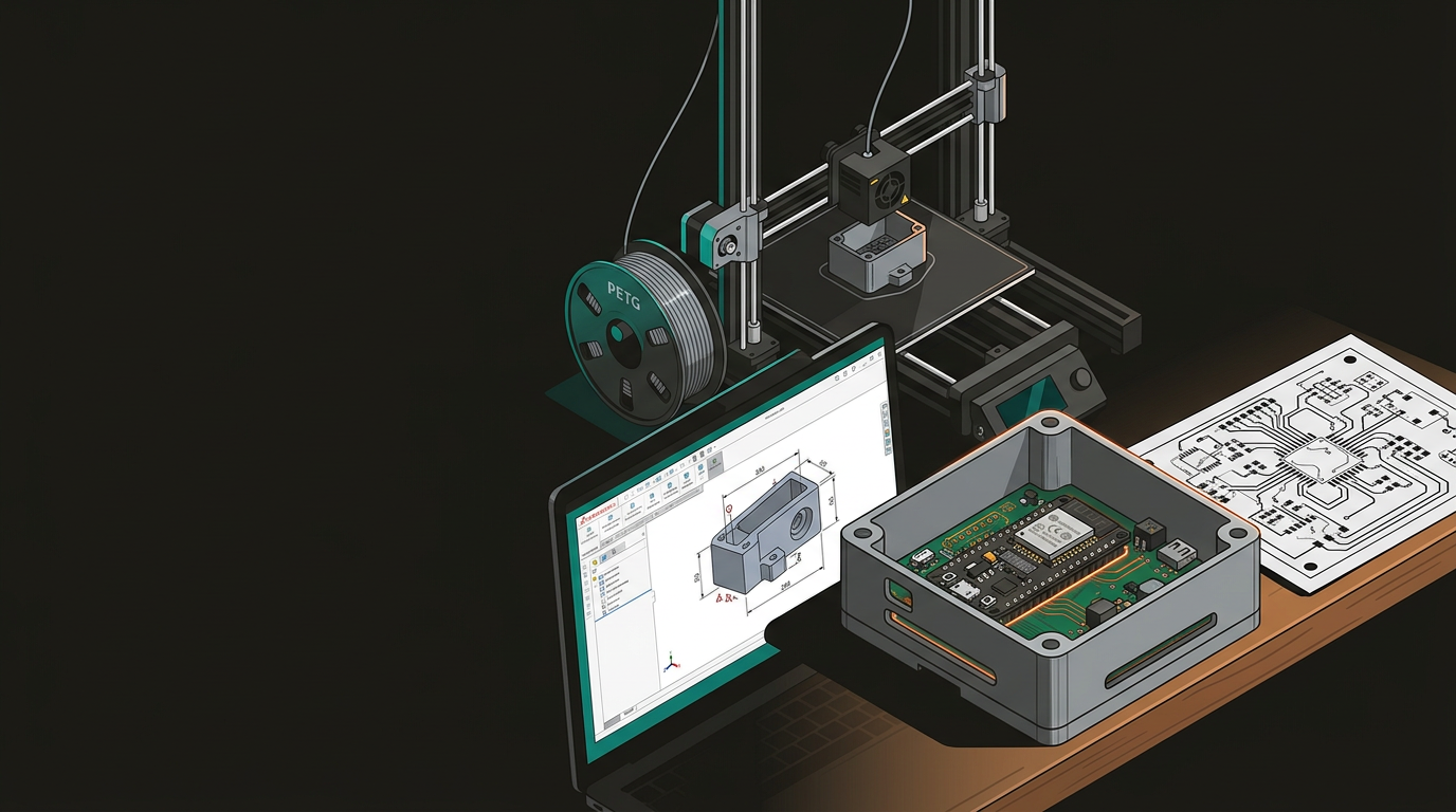
Rapid Prototyping: Where Physical and Digital Meet
Your first physical prototype shouldn’t look like a finished product — it should be the fastest possible way to test assumptions and find where they’re wrong. 3D printing is central to that process for almost every connected hardware project. The choice of method depends on what you need to validate.
FDM — PLA / PETG
- Parts in hand within hours of finalising a CAD revision
- Check fit and test connector clearances with real plugs
- Confirm PCB actually seats where the model says it does
- PETG for better temperature tolerance in field-deployed devices
- Low cost — iterate freely without budget pressure
- First choice for the majority of enclosure validation work
Resin — SLA / MSLA
- Better dimensional accuracy for tight-tolerance features
- Translucent materials for light pipes and sensor windows
- Smoother surface finish for client-facing prototype presentations
- Slower and more expensive than FDM — reserve for specific features
- Post-curing adds time to the iteration loop
- Worth the extra step when clarity or precision is non-negotiable
One discipline that’s easy to skip and consistently painful to ignore: version control your CAD files the same way you version control your code. Every time a design decision changes the enclosure — a connector moves, a vent slot gets added — commit that change with a meaningful description. When a printed prototype has a problem, you need to know exactly which revision you’re holding.
These are the tools that support the rapid iteration loop across disciplines:
Integration Testing: The Stage Most Prototypes Skip
Once you have a physical enclosure with real electronics inside running real firmware, integration testing is where smart prototype development either validates itself or starts unravelling. A structured test works through each layer in sequence — and each layer must be documented against a specific hardware and firmware revision.
Mechanical Fit
Does everything seat correctly, or are cables under stress and connectors slightly misaligned? Physical tolerance issues found at prototype stage cost hours to fix; found after regulatory certification, they cost months.
RF Performance
Run a WiFi or BLE range test with the antenna inside the physical enclosure. Enclosures attenuate RF — sometimes dramatically. You may need to adjust antenna placement or add an external antenna pigtail.
Thermal Behaviour
Run the device at full load in ambient conditions that reflect actual deployment. A thermal camera or thermocouples will find hotspots that look fine on a schematic but cause grief in the field.
Software–Hardware Edge Cases
What happens when the device powers up mid-firmware-update? What’s the behaviour when a sensor fails or returns garbage data? Good firmware thinks through hardware failure modes before they occur in production.
EMC Pre-Compliance
Not full certification, but a sanity check that your device isn’t radiating excessively or misbehaving near other electronics. Essential for any regulated market, including New Zealand’s Radiocommunications Act requirements.
Document every test result against the specific hardware and firmware revision you’re running. That traceability is invaluable when a bug surfaces and you need to establish whether a hardware change or a firmware regression introduced it.
Case Study: Connected Air Quality Monitor
To make this concrete: a compact air quality monitor for deployment across multiple commercial buildings — a real category being developed across New Zealand right now. The same integrated workflow described above, applied to a specific product.
Custom PCB built around an ESP32-S3 module, integrating PM2.5, CO₂, temperature, and humidity sensors. Power via USB-C with a small LiPo backup for outage tolerance.
Designed in Fusion 360 around the PCB outline and sensor placement requirements. Carefully modelled inlet and outlet vents for clean airflow — not a generic slot pattern. Wall-mount bracket integrated into the rear shell, not bolted on as an afterthought.
ESP-IDF with FreeRTOS tasks handling sensor polling, local data buffering, and MQTT publishing. Node-RED aggregates data from multiple deployed units and routes alerts via MQTT → webhook → Slack.
The first PETG enclosure iteration revealed the PM2.5 sensor inlet was being partially blocked by a PCB component that had shifted during final layout. Two hours of CAD work and another print resolved it. In a traditionally siloed project, that discovery easily costs several days of inter-team back-and-forth — and surfaces much later in the process when it’s harder to fix.
GeoSaffer is one of the few Auckland-based operations that spans CAD-informed fabrication — laser cutting, CNC routing, and 3D printing through Plastixel — alongside embedded systems consulting and software development. Whether you’re at the napkin-sketch stage or you already have a CAD file and a BOM ready to move on, the most useful next step is a conversation before you commit to any particular approach.
Talk to the GeoSaffer team →